Semiconductor Cleanroom Design Requirements
- 2024-01-03
- View 21
Imagine life without electronic devices. There would be no TVs, computers, cell phones, smart technology and the list goes on. Today’s developments in the semiconductor market place raise the bar for fabrication efficiency, and companies are looking to build more effective and sustainable production environments.
.jpg)
Before we dive into cleanroom considerations for these applications, let's review semiconductors and the critical environments they are manufactured in.
So, what is a semiconductor?
Semiconductors are materials which have a conductivity between conductors (typically metals) and nonconductors or insulators (such as ceramics). They are typically referred to as integrated circuits or microchips and are made from pure elements such as silicon or germanium, or compounds such as gallium arsenide. Semiconductors are an essential component enabling advancements in renewable energy, healthcare, clean energy, and other applications.
What is a semiconductor fab?
A semiconductor fab is a manufacturing plant in which raw silicon wafers are turned into integrated circuits. Photolithography is a common manufacturing process inside of the cleanroom. This process involves photographing the circuit pattern on a photosensitive substrate and chemically etching away the background. Types of chips manufactured in a semiconductor fab are:
· NAND flash
· DRAM for memory
· Microprocessor
· Graphics controller
· Hard drive controller
· RAID controller
Once completed, these chips go into a wide range of devices such as computers, mobile phones, televisions, laptops, drones, military equipment, and automobiles.
Typical Semiconductor Cleanroom Considerations
Chip manufacturers face a variety of challenges when designing and operating a semiconductor cleanroom Extremely detailed processes and controlled environments are essential to produce wafers. When one speck of dust can destroy the functionality of a chip, the only way to avoid contamination is to control the environment.
Knowing this, facilities lean towards a higher classification to reduce risk of production issues and product failure. One of the main sources of contamination is human workers inside the semiconductor fab. Workers can create unwanted ESD (electrostatic discharge) that can destroy delicate electronic circuits. Other potential contamination occurrences are:
· Glitch in power
· Fan motor breaking
· Pressure malfunction
· Dropping equipment, tools, and parts
· Wafer handling equipment can malfunction
Semiconductor cleanroom environments must be engineered to control static, particulate matter, outgassing, and other sources of contamination and compromising conditions. Environmental control is critical and maintaining the required levels of air purity is a non-negotiable for total performance of the cleanroom. To help maintain air purity, fabs utilize filters at the ambient air inlet (make-up air handler, MUA), often in the return air handlers (RAH) and on top of cleanroom ceiling fan filter units (FFU).
Airflow arrangements is another critical factor in a semiconductor fab. Vertical laminar flow is common inside cleanrooms. This is when air is blown from the ceiling down to the floor, creating a constant, uniform stream if air. Once the air reaches the raised access floor, it flows through the holes in the flooring passing upward through the air plenum to be purified through HEPA filters. The return air is then conditioned to control its temperature and humidity before it is cycled through the cleanroom again. When designing your cleanroom, you want to make sure that the airflow is affected as little as possible so that particles do not build up on any equipment.
What are other considerations?
Some other semiconductor fab considerations are furniture/equipment layout inside of the room. A typical design recommendation for equipment layout is to place the equipment along the outer walls avoiding areas where maximum airflow occurs. Wet benches where workers manipulate the wafers should also be positioned along the cleanroom walls.
High power exhausts built into any wet bench work areas extracting the chemical vapors generated during the manufacturing process should do so without disrupting air flow. You will also see wire racks and shelves inside of semiconductor fabs. This is for maximizing the airflow by eliminating flat surfaces where particles can collect. Wall surfaces in the cleanroom use a special design such as smooth aluminum wall surfaces to help keep air moving.
What classifications of semiconductor cleanrooms do we need?
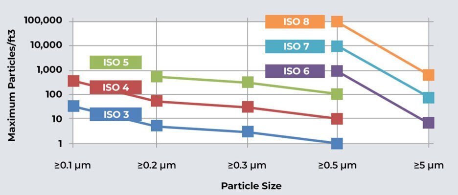
Semiconductor fabs follow the ISO 14644 standard. Specification for device fabrication cleanrooms vary based on process type, line width, and wafer size requirements. Semiconductor cleanrooms requirements can range from ISO 4 (Class 10) to ISO 6 (Class 1,000) cleanrooms.

Certain operations may have an ISO 7 Class (10,000) or ISO 8Class (100,000) background, but all considerations are handled on a project-by-project basis.
Kwang Cleanroom is proud to offer examples of a variety of our cleanroom projects below. Electronics Assembly Cleanrooms, Cosmetic Production Cleanrooms, Automotive Cleanrooms, Aerospace Cleanrooms, Medical Device Cleanrooms, Pharmaceutical & Biotechnology Cleanrooms, Powder Coating Cleanrooms.
